DESCRIPTION
Contains information about building a small radio transmitter, which has a PCB 1.75" x 2.5" (45mm x 68 mm) and has a range of about 30 yards or so. The documentation with the circuit says the freq range is 100-108 MHz, but I have found it to be more like 85-100 MHz.
The circuit is (of course) only mono, and accepts an audio input from either a microphone or other source. The input impedance is 1Mohm. The input sensitivity is 5mV and the max input signal is 10mV. The transmitted signal can be picked up on a FM radio. The circuit can be used for short-range transmission, eg. for wireless microphones.
The actual circuit comes from a 'Kit', available from Veleman electronics (USA distributor is Tapto Corp., PO Box 1339, CLAREMONT NH-03743-US. UK distributor is High-Q Electronics, 382 Edgware Road, London, W2 1EB). The kit number is K1771. It is a very good transmitter.
I bought the kit, and made the circuit, which worked very well. I wanted two transmitters, so I made my own 'copy' PCB and built the circuit, and in fact my home-made version seems to work better than the original!! So there is no need to buy the kit really, as it is quite a simple circuit, and is the best 'home-made' transmitter I have seen.
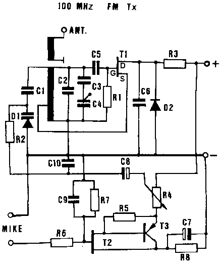
CIRCUIT.GIF is the circuit diagram.
PCBPLAN.GIF shows the PCB layout from above (components shown). PCBPLAN.GIF is an accurate layout, scanned from the instruction sheet. I have used * to mark one corner for reference.
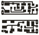
TRACKS.GIF shows the track layout on the soldering side of the board. This is NOT a very accurate layout. This is because I didn't actually have a plan of the track layout. To get TRACKS.GIF, I put a bit of OHP film onto the bottom of the PCB, and traced the tracks with an OHP pen. I then scanned this in. I have marked the component leg holes (approximately) with white blobs.
CONSTRUCTION
Start off by scaling PCBPLAN.GIF and TRACKS.GIF by the same amount so that they measure approximately the correct size (1.75" x 2.5") when printed out.
Then make your PCB. As mentioned earlier, PCBPLAN.GIF gives the accurate positioning of the holes, whereas TRACKS.GIF gives the positions only approximately. So use PCBPLAN when drilling the holes in your PCB board. Then draw on the tracks, using TRACKS.GIF as a guide. The important thing is to make sure you draw the 'printed coil' correctly on the PCB - those lines are there for a reason!
Parts
D1 Varicap diode (eg. BB119)
D2 1N4148
R1 100K
R2 220K
R3 22R
R4 1K trimmer
R5 1K
R6 56K
R7 1M
R8 1K2
C1 5pF ceramic
C2 6pF ceramic
C3 15pF ceramic
C4 trimmer cap
C5 15pF ceramic
C6 1nF ceramic
C7 100uF electrolytic
C8 4.7uF electrolytic
C9 100pF ceramic
T1 BF244A or BF245A FET
T2 2N3819 FET
T3 BC307/8/9 or BC557/8/9 PNP
Bear in mind that in addition to the components, there is a jumper wire which needs to be fitted (marked with a dashed line in PCBPLAN.GIF).
The power supply to use is 9-14 V DC, one of the little rectangular 9V batteries is fine. Connect this to the + and - points on the PCB. The sound input goes to the points marked "MIKE". The antenna should be connected to the point marked "ANT". The emitter's output impedance is 50 ohms. You can make your own fancy antenna if you like, but I have found that a foot or so of wire is fine.
Good luck with the transmitter. If you have any improvements to the circuit, I would be glad to hear from you. --Dan Evans.
Author: Dan Evans
Email: dan.evans@sjc.ox.ac.uk
Website: http://sable.ox.ac.uk/~sjoh0014/web/dan.html

 Audio
Audio


